Electronic device manufacturers must meet tight tolerances and maintain complex part geometries. Screen glass defects, pin misalignments, circuit board deformation, and other issues not only affect product quality, but also increase consumer safety risks.
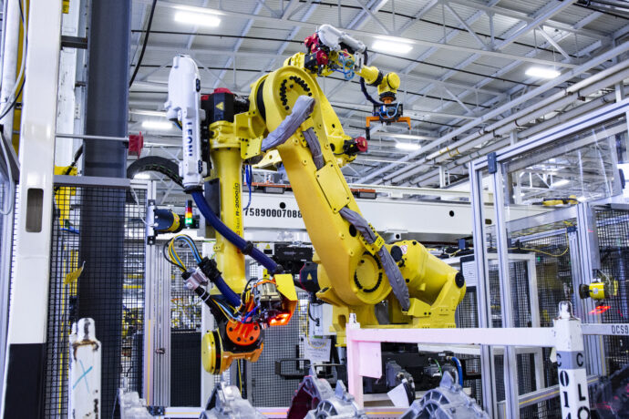
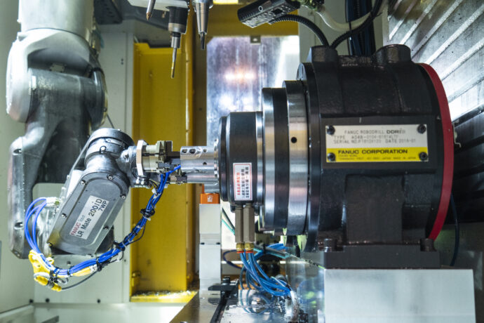
Implementing 3D automated metrology systems is one way to overcome electronic device manufacturing challenges. Automated systems are both fast and precise, and can help identify and mitigate product defects in real-time, during any stage of the manufacturing process.
If you’re new to automated metrology, MAS is here to help. We specialize in helping electronic device manufacturers build and implement custom automated metrology systems. Read on to learn more about our metrology solutions and capabilities.
MAS offers 3D automated metrology solutions that can be used in a wide range of applications across multiple industries, including electronic device manufacturing and quality control. For businesses in electronics markets, MAS’ metrology systems can assist with chip inspection, smartphone component inspections, scanning and identification of PCB components, PCB assembly inspections, and adaptive assembly of high-precision electrical connections.
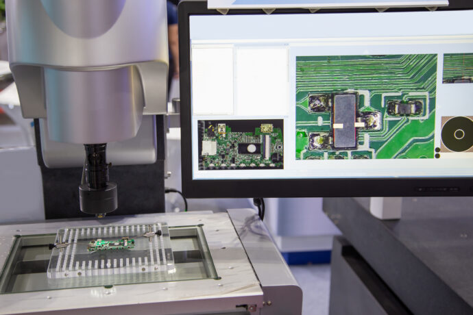
Our QC Plus™ 3D metrology scanners have advanced chip and substrate metrology and inspection capabilities. This allows chip manufacturers to perform high-volume manufacturing process monitoring, and even characterize new processes to obtain real-time data and inspect feasibility. These metrology scanners can also provide precise measurement data for film thicknesses, pattern placement, layer-to-layer alignments, surface topography, pattern dimensions, and more.
Our automated metrology systems are capable of performing smartphone component inspections, including the non-invasive inspections of body housings, camera and lens components, and glass housings. Precise measurement data can be obtained that characterizes coating coverage, coating thicknesses, and step heights. Additionally, these measurements can be used to inspect for gaps and scratches in smartphones during the production process. For micro-components such as smartphone camera objective lens assemblies, our 3D metrology scanners can also be used to ensure precise positioning of lens components to achieve crystal clear, sharp, and distortion-free images in the end product.
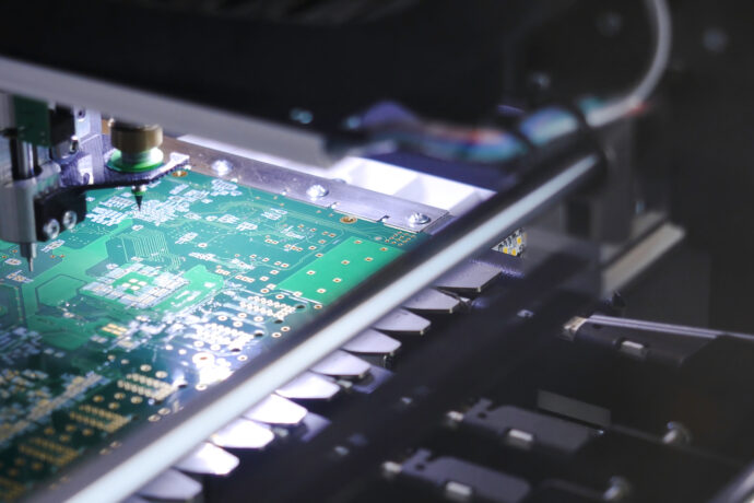
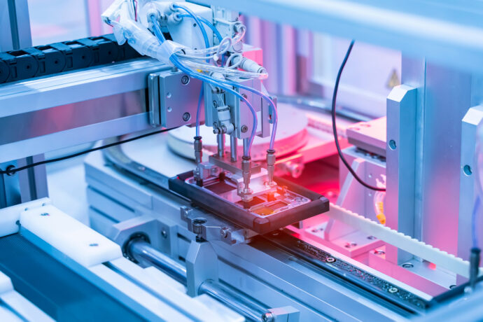
Our metrology solutions also include scanning and identification of printed circuit board (PCB) circuitry, decal placements, sticker placements, and even high-concentration features such as mesh and pin holes. While manual measurements are always an option, automated measurement routines can also be used to automatically inspect a variety of GD&T measurements.
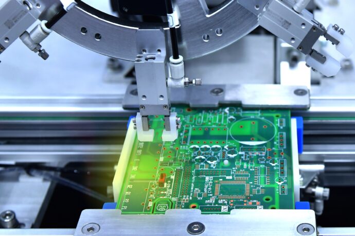
MAS has innovated Scan-to-Path™ software that enables adaptive control within manufacturing and assembly processes based on high resolution measurement data. For example, our Scan-to-Path™ enabled measurement systems can measure the housing, then rework out of tolerance areas. Or the system could adaptively place components to fit perfectly in that part’s housing. QC Plus™ metrology with Scan-to-Path ™ software allows you to reduce and even eliminate human error and time-intensive quality control bottlenecks.
Request a meeting with one of our experts today to discuss your needs.
We want to hear about how we can customize our products for your requirements.